




A smartphone has a chip inside it that seems too small to matter. If you set it beside a grain of rice, it still feels like it could not possibly help with an AI task, handle video, steer an electric car, or keep a modern computer running. And yet inside that little bit of silicon there are a huge number of tiny parts. They are lined up with extreme care, far more exact than you would guess just by looking at it.
That is what makes the microchip fabrication process so difficult to understand at first. It is not one manufacturing step. It is a long chain of processes where manufacturers repeatedly add material, remove material, change the properties of the silicon, create patterns, build connections, test everything, and finally package the finished dies. A mistake in one stage can follow the chip all the way to the end.
So, how does a piece of silicon actually become a working microchip? The answer starts with a wafer and ends with a very different idea of what ‘packaging’ even means.

The Foundation of Silicon Wafers and Zero-Dust Cleanrooms
Silicon is not used simply because it is available in large quantities. Its real value comes from the way it behaves electrically. Under controlled conditions, manufacturers can change how silicon conducts electricity. That makes it possible to build the switching elements that form the basic logic of modern electronics.
The raw material first has to go through extensive purification. Semiconductor manufacturing needs extremely pure silicon, so manufacturers process the material and form it into cylindrical silicon ingots. Those ingots are then sliced into thin, flat wafers.
At this point, there is no computer hiding inside the wafer. It is basically a blank surface waiting for its circuit to be built.
This is where the microchip fabrication process starts getting difficult. The wafer will go through many rounds of processing. Materials will be deposited onto it. Some will stay. Some will be removed. Certain areas will have their electrical properties changed. Patterns will be created and then transferred into the layers underneath. And this keeps happening until the circuit starts taking shape.
The setting is not optional. In a semiconductor fab, everything is run inside a clean room with strict controls. Dirt that would be harmless in daily life can still wreck tiny structures. When the part is being made at a scale far below what people can see, even a small speck can turn into a serious flaw.
The wafer therefore has to remain clean while all this work happens. Precision is not a nice extra here. It is the foundation of the entire semiconductor fabrication process.
The Front-End Fabrication Process and Building the Circuit
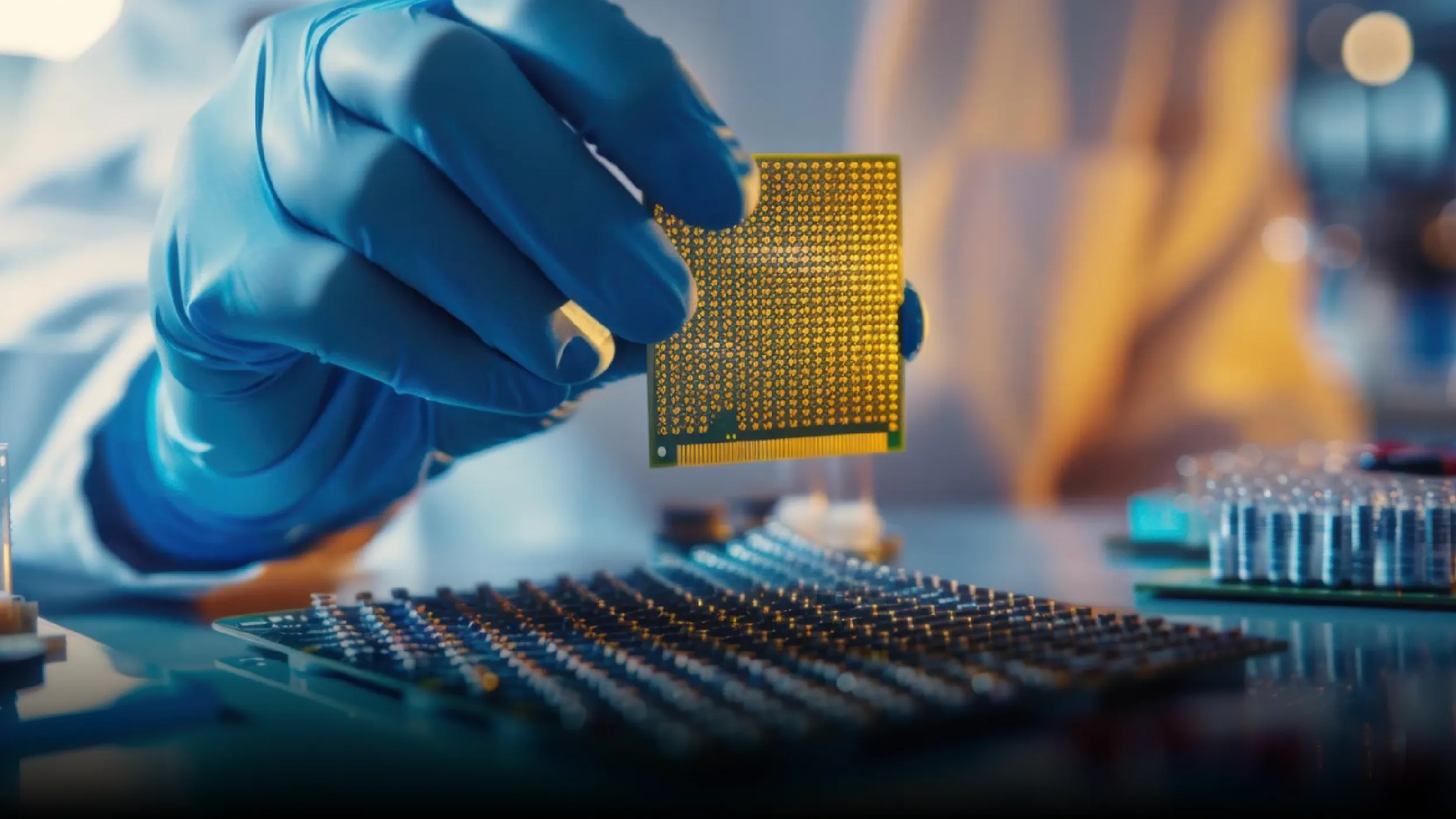
This is the part where the wafer starts turning into an actual electronic device. There is no single moment when a transistor suddenly appears. Instead, manufacturers build the structure through repeated cycles of deposition, patterning, etching, doping, cleaning, and other processes.
Thin-Film Deposition
The first task is often to put a very thin layer of material onto the wafer. The material might provide insulation, conduct electricity, or serve as part of a structure that will be shaped later.
Two techniques that appear in semiconductor manufacturing are chemical vapor deposition, or CVD, and physical vapor deposition, or PVD. The names sound complicated, but the basic idea is fairly simple. Manufacturers need to place a specific material onto the wafer with very tight control over where it goes and how thick the layer becomes.
Then they do it again.
And again.
That repetition is one of the less obvious realities of the microchip fabrication process. A modern chip is not built by creating the entire circuit at once. It grows through many carefully controlled layers, with every new layer having to work with what came before it.
Photolithography and the Most Critical Step
Now comes one of the most important parts of the process. Photolithography decides where the next structures will be created.
Manufacturers coat the wafer with a light-sensitive material called photoresist. They then expose it to a carefully controlled pattern of light. The exposed areas of the photoresist change, allowing manufacturers to develop a pattern on the wafer.
That pattern acts like a temporary guide. The next steps use it to determine which parts of the underlying material should stay and which should go.
It sounds straightforward until you consider the scale.
Also Read: What Is the Future of Driverless Truck Technology and How Will Autonomous Trucks Transform Logistics?
The industry keeps trying to make transistor features smaller. As those features shrink, the pattern itself becomes harder to print accurately. This is why lithography has become such a major battlefield in advanced semiconductor manufacturing.
Extreme ultraviolet, or EUV, technology plays a major role at the leading edge. EUV uses a much shorter wavelength than older lithography approaches, allowing relevant patterns to be produced with fewer patterning steps.
ASML’s High-NA EUV platform pushes this further. The company says it increases numerical aperture from 0.33 to 0.55 and is designed to support geometric chip scaling beyond the next decade, starting with the 2nm logic generation and later memory nodes at similar transistor densities.
There is also a useful reality check here. This is not technology sitting in a research lab waiting for someone to figure out what to do with it. In July 2026, ASML reported that Intel Foundry entered high-volume manufacturing for a subset of Core Ultra Series 3 processors using ASML’s EXE High-NA EUV technology. Specific Intel 18A layers had also been dual-qualified on High-NA EUV in Oregon.
That matters because it shows where the microchip fabrication process is heading in practice. The smaller the features become, the more demanding the equipment becomes too.
Etching
Printing the pattern is only half the job. The manufacturer now has to transfer that pattern into the material underneath.
That is where etching comes in.
Depending on the material and structure involved, manufacturers can use gases or chemicals to remove selected areas. The goal is not simply to remove material. It is to remove the correct material from the correct places while leaving the rest of the structure intact.
This becomes particularly important when manufacturers create three-dimensional transistor structures. A transistor is no longer just a flat shape sitting on top of the silicon. Modern designs use carefully formed structures that interact with the electrical field in much more controlled ways.
The microchip fabrication process therefore involves an interesting contradiction. Manufacturers are constantly trying to make things smaller, but the physical structures still need to be shaped accurately in three dimensions. Smaller does not mean simpler. Usually, it means the opposite.
Doping and Ion Implantation
Silicon needs another change before it can perform useful transistor functions. Manufacturers alter its electrical properties by introducing controlled amounts of other elements. This process is called doping.
Ion implantation is one technique used for this. Manufacturers accelerate ions and implant them into selected regions of the silicon. Those regions then behave differently electrically.
This helps create the conditions needed for transistor operation, including the P-type and N-type regions used in semiconductor devices.
People think older chips use simple transistor layouts, but today’s designs are not like that. Intel’s 18A process is a newer step. It uses RibbonFET, which is a gate-all-around idea. In this setup, the gate wraps around the channel. Intel says this gives better control of the electric field. It also helps the design move past what FinFET handled before. Intel also adds PowerVia, power that comes from the back side.
That distinction matters. Semiconductor progress is not simply a race to make the same transistor smaller. At some point, the structure itself has to change. The microchip fabrication process evolves because the old approach eventually runs into physical and engineering limits.
Back-End Manufacturing and Wiring, Testing, and Packaging
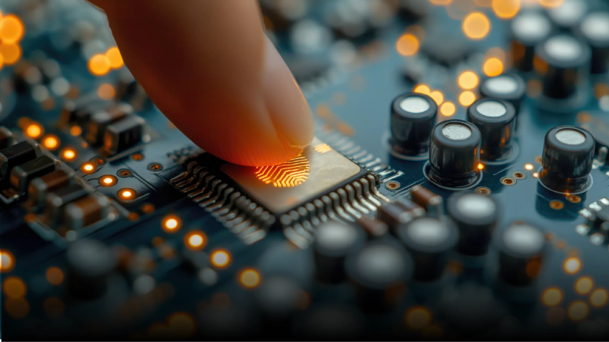
Getting the transistor structures right does not mean the chip is finished. Far from it.
Those transistors need to communicate. They need power. The finished devices need testing. Then the wafer has to be separated into individual dies and connected to the rest of the system.
Metallization and Interconnects
The next major task involves building the microscopic wiring that connects different parts of the circuit.
Manufacturers create layers of conductive material that form interconnects between transistors and other circuit elements. Copper and other conductive materials can be used for these connections.
This is another part of the microchip fabrication process where scale creates the real challenge. A modern chip can contain an enormous network of microscopic connections, all packed into a tiny area. Those connections have to carry signals and power without creating problems that undermine the rest of the circuit.
The transistor gets most of the attention because it sounds more impressive. In reality, a transistor that cannot communicate with the rest of the chip is not particularly useful.
Wafer Testing and Dicing
Before the wafer is cut apart, manufacturers test the devices built on it. Electrical probing can identify areas that do not behave as expected and help manufacturers determine which dies are suitable for further use.
Testing is becoming more complicated as chip designs become more complicated. Intel says its advanced chiplet test methodology identifies known-good dies, while system-level testing can detect marginal defects that traditional testing may miss.
Once testing is complete, the wafer can be diced into individual pieces. Each piece is called a die. That die contains the actual circuit, but it still needs a way to connect with the wider system.
Advanced Packaging
This is where the old definition of a chip package starts falling apart.
Packaging used to be easy to explain. Put the chip inside a protective structure, provide electrical connections, and keep it safe. At the leading edge, packaging is becoming part of the performance story itself.
TSMC’s CoWoS technology is a good example. The company says CoWoS integrates multiple system-on-chip dies with high-bandwidth memory stacks. Its CoWoS-S approach uses a silicon interposer and high-density interconnects to bring logic chiplets and HBM cubes together in the same package.
That is a very different proposition from simply protecting a single die.
With 2.5D and 3D approaches, manufacturers can place multiple dies close together and connect them in ways that would be difficult or impossible if everything had to fit onto one piece of silicon. The microchip fabrication process has therefore expanded beyond the wafer itself. How the dies are assembled can now influence what the final system is capable of doing.
How Microchip Fabrication Enables the AI Era
This is where all those manufacturing steps finally connect to something people actually notice.
AI hardware needs huge amounts of computing power, but compute is only one side of the problem. Data has to move between processors and memory quickly. If that movement becomes a bottleneck, adding more computing power does not magically solve the problem.
This is why advanced packaging and high-bandwidth memory have become so important.
Samsung says its HBM4 uses 12-layer stacking, with capacities ranging from 24GB to 36GB, while a 16-layer configuration is planned to reach up to 48GB. Samsung also says HBM4 can deliver up to 3.3 TB/s of bandwidth per stack, representing a 2.7x increase over HBM3E.
That puts the role of packaging into perspective. Logic and memory can be brought much closer together, allowing data to move between them at very high speeds. The physical arrangement of the components becomes part of the computing architecture.
So the microchip fabrication process is not just about squeezing more transistors into less space. It is about improving the entire chain. Better lithography creates finer patterns. New transistor structures improve control. Interconnects move signals and power. Packaging brings dies together. High-bandwidth memory keeps data moving.
For AI, that combination matters more than any single breakthrough.
Conclusion
The interesting part of the microchip fabrication process is not that manufacturers can turn silicon into a computer. It is how many things have to go right before that computer can do anything at all.
The industry has spent decades making features smaller. That still matters, but it is no longer the whole story. The pressure has moved across the entire manufacturing chain. Lithography has to become more capable. Transistors need new structures. Power delivery needs smarter solutions. Packaging has become part of system design. Memory has to keep pace with increasingly demanding workloads.
That changes how we should think about semiconductor scaling. The future will not be won simply by whoever makes the smallest transistor. It will belong to the companies that can make the wafer, transistor, power network, memory and package work together without one becoming the bottleneck for everything else.