


Semiconductors are probably something you’ve heard about. The use of semiconductors is truly everywhere. Although most people have heard of semiconductor usage, very few are actually knowledgeable about them.
We intend on changing that.
Take this as your guide to the world of semiconductors. By the time you’ve finished reading this article, you’ll be familiar with the use of semiconductors and how to make semiconductors.
What are Semiconductors and How Do They Power Our World?
A semiconductor is a material that is used in electronic equipment and devices to manage and control the flow of electricity. It either prevents a free-flowing electric current from occurring or entirely repels the current.
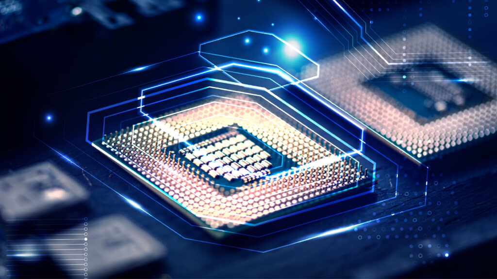
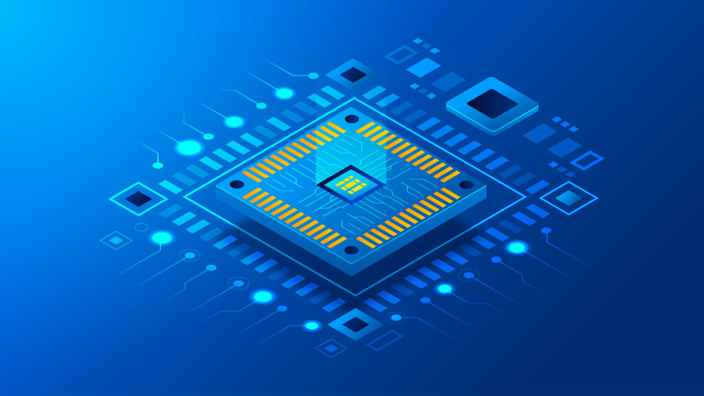
The primary use of semiconductors is in the creation of electronic chips, computing components, and devices that lie between a conductor and an insulator. Having said that, silicon, germanium, or other pure elements are generally utilized in its creation.
By introducing impurities to these elements, semiconductors are manufactured. Depending on the type and quantity of additional impurities, an element’s conductance or inductance will change.
Semiconductors can be divided into two categories such as N-type semiconductors and P-type semiconductors. When a semiconductor’s conductance is higher or there are a lot of free electrons, an N-type semiconductor is used. When there are fewer free electrons and a larger inductance in the semiconductor, a P-type semiconductor is utilized.
Computer memory, integrated circuits, diodes, and transistors are examples of conventional devices and components created with the use of semiconductors.
Now that we are familiar with what a semiconductor is and the use of semiconductors, let’s learn more about how to make semiconductors.
From Sand to Silicon: An Intricate Semiconductor Manufacturing Process
You already know how effective today’s digital devices are such as computers, smartphones, gaming consoles, and more. Microchips, some of the smallest but most intricate pieces of technology ever created, provide most of this power with the use of semiconductors. There are numerous microchips everywhere: Around the world, more than a trillion microchips were produced in 2020. Every individual on the planet amounts to around 130 chips. However, despite what their ubiquitous use might imply, creating a microchip is in no way an easy task.
Its effect on supply chains, economic crises, and intermittent inflationary constraints also raised the question why is there a global shortage of semiconductors?
The use of semiconductors in the creation of chips has played an important role. Numerous semiconductor manufacturing processes are used to create chips. Let’s talk about six crucial steps in the semiconductor production process.
- Deposition
A silicon wafer serves as the process’ foundation. The 99.99% pure silicon bar known as an “ingot” is cut into wafers and polished to an incredibly flawless finish. Depending on the type of structure being created, thin films of conducting, isolating, or semiconducting materials are deposited on the wafer to prepare it for printing the initial layer. This crucial step is frequently referred to as “deposition.”
The “shrinking” of microchip architecture makes the wafer patterning process even more difficult. Deposition, etch, and lithography advancements are key processes to shrink.
- Photoresist coating
The wafer is subsequently covered with a “photoresist,” or simply “resist,” layer that is light-sensitive. There are two types of resist such as positive and negative.
The chemical composition of the substance and how the resist responds to light are the fundamental distinctions between positive and negative resist. Positive resists causes the portions that are exposed to UV radiation to alter structurally and become more soluble, making them ready for etching and depositing. Negative resists, on the other hand, results in sections exposed to light polymerizing, which makes them more durable and challenging to dissolve. Positive resist is most frequently utilized in the semiconductor production process due to its superior lithography stage performance and higher resolution capacity.
The Dow Chemical Company, JSR Corporation, Fujifilm Electronics Materials, and other businesses all around the world make resists for the production of semiconductors.
- Lithography
As it defines how small the transistors on a chip can be, lithography is an important step in the chip-making process. The chip wafer is put into lithography equipment at this stage and subjected to deep ultraviolet (DUV) or extreme ultraviolet (EUV) radiation. Light having a wavelength ranging from 365 nm to 13.5 nm, for simpler chip designs, is used to create the finest details in the chip, some of which are thousands of times smaller than a grain of sand in size.
The “reticle,” which contains the blueprint for the pattern to be printed, projects light onto the wafer. The pattern is condensed and focused onto the resist layer by the system’s optics (lenses in a DUV system and mirrors in a EUV system). As was previously said, when light strikes the resist, it undergoes a chemical shift that allows it to copy the reticle’s pattern onto the resist layer.
It’s difficult to get the pattern exactly correct each time. This process is susceptible to physical or chemical flaws such as particle interference, refraction, and others. Due to this, the pattern sometimes needs to be optimized by purposefully deforming the blueprint, leaving you with the precise pattern that you require.
- Etch
To exhibit the desired pattern, the degraded resist must be removed next. The wafer is baked, developed, and some resists are washed away during the etching process, revealing a 3D pattern of open channels. The chip structure’s general integrity and stability must be maintained while accurately and consistently forming increasingly conductive features. Chipmakers are now able to use double, quadruple, and spacer-based patterning to manufacture the smallest features of the most recent chip designs. This is greatly aided by advanced etch technology.
Both resist and etch come in wet and dry varieties. In dry etching, gases are used to specify the exposed pattern on the wafer. On the other hand, in wet etching, chemical baths are used to wash the wafer. Semiconductor etching systems are produced by businesses including Lam Research, Oxford Instruments, and SEMES.
- Ion implantation
The wafer may be bombarded with positive or negative ions after patterns have been etched on it to adjust how well some of the patterns conduct electricity. The raw silicon used to make the wafer is not a perfect conductor or insulator. The electrical characteristics of silicon fall somewhere in the middle. Transistors, the electronic switches that serve as the fundamental building blocks of microchips, can be made by directing electrically charged ions into the silicon crystal. Thus, this entire process is known as “Ion implantation”.
- Packaging
From design to production, the complete process of producing a silicon wafer with functional chips entails thousands of processes and can take longer than three months. The wafer is cut into individual chips using a diamond saw in order to remove the chips from it. These so-called “dies,” which are sliced from a 300-mm wafer, the size which is most frequently utilized in the semiconductor industry, vary in size for different chips. While some wafers only have a few dozen chips, however, others can have thousands.
After that, a “substrate” is put on top of the chip die. This particular baseboard for the microchip die uses metal foils to direct the chip’s input and output signals to different system components. A “heat spreader” is placed on top to secure the lid. The microprocessor is kept cold while operating due to the heat spreader, a small, flat metal container that serves as protection.
Wiliot, Ayar Labs, SPTS Technologies, and Applied Materials are just a few of the many companies in the semiconductor packaging industry.
Just the Beginning
Now that it is a part of your smartphone, TV, tablet, or other electronic devices, the microchip is all set to incorporate into these devices with the use of semiconductors. Despite being only slightly larger than your thumb, a chip can house billions of transistors. The A15 Bionic system-on-a-chip from Apple, for instance, has 15 billion transistors and can do 15.8 trillion operations per second.
Of course, when it comes to the use of semiconductors and their manufacturing process, there are a lot more steps involved than simply these. Additional processes include testing, electroplating, measuring, and inspection. Additionally, before a microchip is used in a device, it undergoes this procedure hundreds of times.