


Semiconductor fabrication, often referred to as semiconductor manufacturing or simply “fab”, stands as the bedrock of modern electronics. It’s the intricate process that transforms raw silicon wafers into the microchips that power our computers, smartphones, and an array of electronic devices we rely on daily.
This engineering marvel involves a symphony of precision, innovation, and cutting-edge technologies. Let’s talk more about this procedure in detail, exploring its intricacies, and the pivotal role it plays in shaping our technological landscape.
What is Semiconductor Fabrication?
Having a strong grasp of the fundamental characteristics of semiconductors is crucial before delving into the intricate realm of semiconductor fabrication.
Semiconductors are materials that possess electrical conductivity and resistivity characteristics that lie between those of conductors and insulators. In essence, a semiconductor can be defined as a device that enables the flow of current when a voltage is applied. The energy gap found in semiconductor materials falls within the range of approximately 2-3 eV, sitting between conductors and insulators. The distinct electrical properties of semiconductors make them highly suitable for utilization in various electronic devices.
Semiconductor Fabrication Process
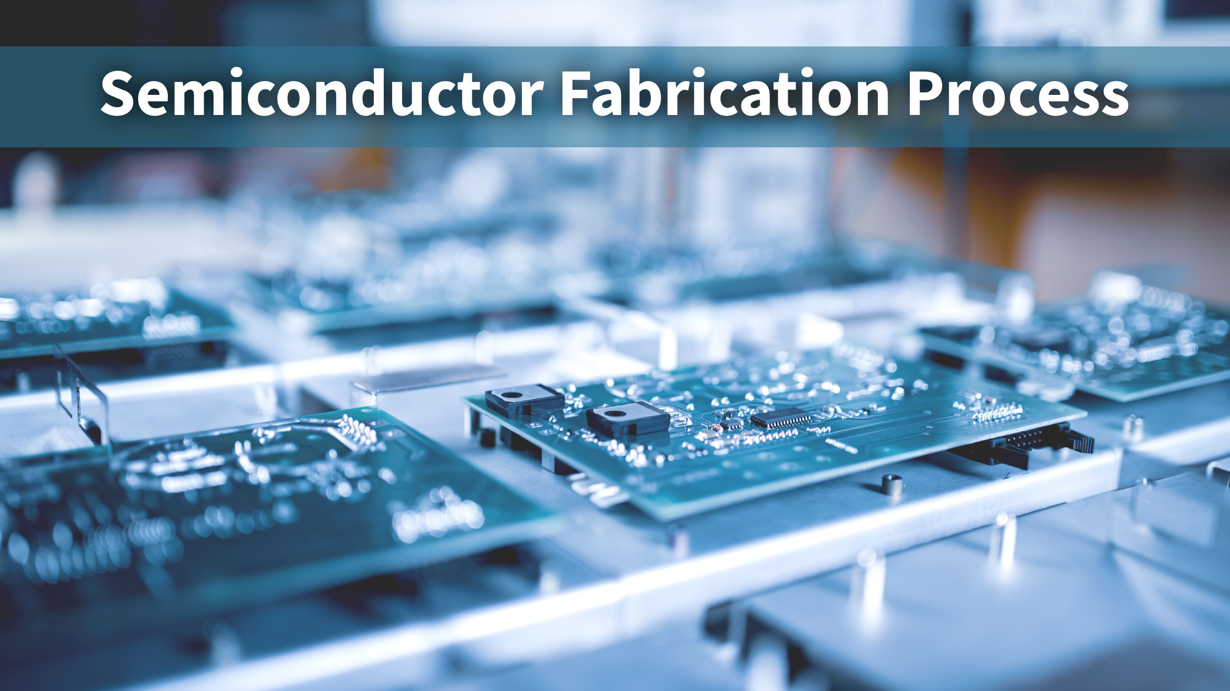
The steps involved in this complex process of semiconductor fab and IC manufacturing are detailed below.
Step 1: Build the silicon wafer
The first crucial step in the semiconductor fabrication process involves creating silicon wafers that have intricate circuit patterns engraved multiple times onto selected materials. Afterwards, these wafers undergo polishing to ensure uniformity.
Step 2: Imprint the Integrated Circuit (IC)
Photolithography is a process used to transfer complex designs onto a silicon wafer. The wafer, which is covered in a light-sensitive substance, is subjected to ultraviolet (UV) light while being shielded by a mask. This method allows for the efficient creation of accurate and consistent shapes.
Step 3: Etch the plasma
The resist pattern is transferred through plasma etching after lithography. This efficient semiconductor fabrication procedure involves modifying the properties of the plasma through gas discharge to achieve precise etching. Another option is wet-chemical etching, a less expensive liquid-based method primarily utilized for larger geometries with fast diffusion rates.
Step 4: Create the thin film
A thin film forms by depositing materials atomically or molecularly. Methods like physical or chemical vapor deposition are employed for this purpose. It contains both conductive metal layers and non-conductive insulating layers.
Step 5: Interconnect metals
After forming the thin film, fine gas particles deposit ions, giving the semiconductor electric properties. Metal circuits, typically aluminum or copper, connect electronic elements, enabling signal transmission.
Step 6: Conduct electrical die sorting
Electrical die sorting (EDS) boosts semiconductor yield by pinpointing defective chips on the wafer. This enhances overall chip production efficiency. During EDS, a probe card with tiny pins makes contact with the wafer, sending electrical signals through. This reveals any defects, which are then marked for repair. If a chip fails after repair, it is discarded. EDS is crucial for saving resources and time in subsequent processes.
Step 7: Package the IC
This step involves cutting wafers into individual chips, placing them on a lead frame for electrical connections, and molding them with heat into the desired external shell.
Step 8: Test the IC
After the packaging process, the IC goes through extensive testing to ensure its proper operation in different conditions. This testing guarantees the quality and functionality of the IC. Once the IC’s performance is confirmed, it is labeled and made ready for sale.
Semiconductor Fabrication Standards
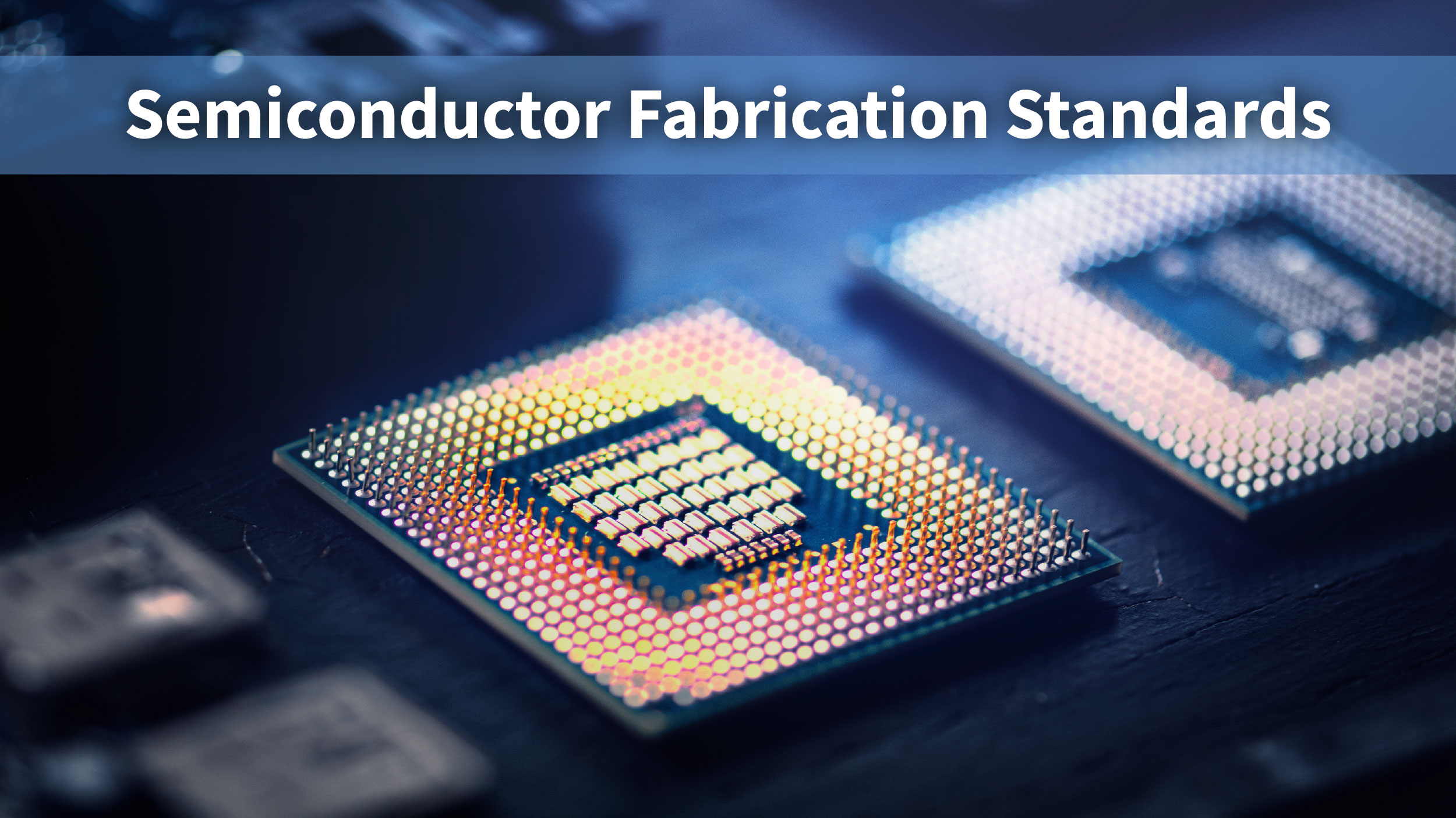
Semiconductor manufacturing standards are guidelines for processes, materials, and safety when making semiconductors, ensuring industry-wide consistency, quality, and safety. Below are essential insights into standards related to semiconductor manufacturing:
- Cleanroom Standards: Cleanrooms are vital in semiconductor manufacturing for a contamination-free environment. Standards regulate air quality, particle counts, and gas distribution. For instance, the International Electrotechnical Commission (IEC) 62258 covers semiconductor die products.
- Safety Standards: Semiconductor manufacturing places a high importance on ensuring safety. Measures such as NFPA 318 standards are put in place to safeguard workers, facilities, and the environment against potential risks, particularly fire-related hazards.
- Environmental Standards: Device fabrication uses chemicals and processes with potential environmental impact. Regulations like National Emission Standards for Hazardous Air Pollutants (NESHAP) control emissions to reduce hazardous pollutants from manufacturing facilities.
- International Standards: International organizations such as the IEC and ISO play a significant role in establishing semiconductor fabrication standards that are adopted worldwide, in addition to national standards.
What are the Future Trends in Semiconductor Fabrication?
The semiconductor sector is continuously changing as a result of technological advancements and market requirements. Here are a few upcoming developments in semiconductor manufacturing:
1. Advanced Process Technologies:
As semiconductor components continue to decrease in size and increase in complexity, innovative methods like extreme ultraviolet lithography (EUV) and multi-patterning are being created to facilitate the production of smaller features and greater transistor densities.
2. More Efficient Transistors:
In the pursuit of enhanced performance and energy efficiency, researchers are investigating new transistor designs and materials. This encompasses novel architectures like FinFET and nanowire transistors, along with alternative channel materials such as III-V compounds and 2D materials like graphene.
3. More Integration and System-on-Chip (SoC) Designs:
In recent times, there has been an increasing inclination towards the incorporation of more features onto a solitary chip. System-on-chip (SoC) designs amalgamate various elements, including processors, memory, and sensors, onto a single chip, resulting in smaller device sizes and reduced energy consumption.
4. Advanced Packaging Technologies:
Semiconductor devices rely on advanced packaging to meet performance demands. Fan-out wafer-level packaging, 2.5D/3D packaging, and chiplet-based packaging are key technologies in development.
5. Internet of Things (IoT) and Edge Computing:
The rise in the number of IoT (Internet of Things) devices and the demand for edge computing are fueling the advancement of specialized semiconductor solutions. These solutions encompass energy-efficient and cost-effective devices designed specifically for IoT applications, along with edge AI accelerators that handle data processing at the network’s edge.
Summing it Up
Semiconductor manufacturing or fab, a cornerstone of modern technology, involves intricate techniques and cutting-edge equipment. These advancements drive innovation in semiconductor fabrication techniques, pushing the boundaries of what’s possible. From clean rooms to photolithography machines, the precision of semiconductor fabrication equipment plays a pivotal role in crafting the powerful microchips that power our digital world. Advancements in semiconductor manufacturing equipment drive technology forward, shaping a future with faster, smaller, and more powerful devices beyond our imagination.